Lithography machine giant ASML is rumored to "leave" the Netherlands, and the Du
The Netherlands has urgently established a special task force, led by Prime Minister Mark Rutte, in an attempt to retain ASML.
According to a report in the Dutch newspaper De Telegraaf on March 6th, a source revealed that due to the Dutch government's inclination towards anti-immigration policies, the lithography giant ASML is planning to relocate out of the Netherlands. In response, the Dutch government has set up a special task force named "Beethoven Plan," personally led by Prime Minister Mark Rutte, to explore methods to prevent ASML from leaving.
The primary factor for ASML's desire to leave the Netherlands is the country's "anti-immigration policy." In November of the previous year, the Dutch Freedom Party gained an overwhelming majority in the parliamentary elections and announced its commitment to advancing anti-immigration policies, reducing the scale of international students, and advocating for a departure from the European Union. ASML employs 40% non-Dutch staff, with significant numbers of international students long-term employed in research and development departments.
Advertisement
In light of these changes, ASML's Chief Executive Officer Peter Wennink stated in January out of concern for the deteriorating business environment in the Netherlands, "The consequences of restricting labor mobility are enormous; we need these people for innovation. If we can't find them here, we will go to other places where we can grow."
In response to recent rumors about "leaving the Netherlands," an ASML spokesperson told the media that they are considering the company's future but did not disclose specific thoughts. Reports suggest that France is one of the potential destinations for ASML.
Additionally, insiders have revealed that the housing shortage in the Netherlands is also a contributing factor to ASML's consideration of relocation. In response to the aforementioned report, an ASML spokesperson replied to De Telegraaf, saying, "It is clear that we must continue to grow. We have received many questions about how to do it, how to do it, and where to do it, but we cannot respond to all the rumors and speculations."
In an interview later on the evening of the 6th, Dutch Minister of Economic Affairs Micky Adriaansens did not respond to the aforementioned report. However, she confirmed that she planned to hold talks with ASML's CEO Wennink in The Hague, the Netherlands, on the same day."I don't know if they will leave the Netherlands," Adriana Stein admitted, "They want to grow, they want to continue to expand, and this goal puts pressure on our infrastructure." She added: "That's why we've had very intense conversations. Because we want to know, can we solve this problem?"
The Telegraph reports that ASML's departure or expansion overseas would be an extremely sensitive blow to the Netherlands. In recent years, concerns about the Dutch business environment are reaching a boiling point, with multinational companies Shell and Unilever having left the Netherlands in succession.
ASML High Numerical Aperture (High NA) EUV Lithography System Achieves "First Exposure"
At the end of February at the SPIE Lithography Conference, Intel's head of technology development, Ann Kelleher, mentioned that they have achieved the "first exposure" milestone on ASML's new high numerical aperture (High NA) EUV lithography system, which ASML also confirmed, stating that they will continue to test and adjust the system to enable it to perform at its full capacity.
So what does "first exposure" mean? "First exposure" refers to the lithography system's first successful projection of light patterns onto a wafer. This signifies that the lithography system has completed its basic functionality verification and can begin further testing.
What is the significance of this progress? The high numerical aperture EUV lithography system is considered one of the key technologies for next-generation chip manufacturing. It can etch finer circuits on smaller chips, enabling the chips to become more powerful and energy-efficient.

ASML's successful achievement of "first exposure" indicates that the company has made significant progress in this key technology. This will facilitate the acceleration of the development process for next-generation chips.
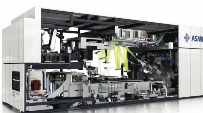
ASML also showcased its next-generation high numerical aperture extreme ultraviolet (EUV) lithography system and revealed that the price of its High-NA Twinscan EXE lithography system is approximately €350 million (currently about 2.737 billion yuan). In comparison, the price of the existing EUV lithography system is about €170 million (currently about 1.329 billion yuan), of course, the specific price depends on the specific model and configuration.
ASML stated that, to date, the company has received "10 to 20" orders from several companies, including Intel and SK Hynix, and plans to produce 20 units per year by 2028.Based on currently available information, major advanced chip manufacturers, including TSMC and Samsung, are expected to introduce this equipment within the next five years. Intel has stated that they plan to use it for the production of the Intel 14A node.
ASML's High-NA Twinscan EXE lithography machine represents the pinnacle of the company's technology. Each unit weighs 150 tons, equivalent to two Airbus A320 aircraft, and requires 250 shipping containers for transportation. Once delivered to the customer, it takes another six months for 250 engineers to assemble it.
The world's first high numerical aperture (NA) equipment is located at the Eindhoven Litho Field Laboratory in the Netherlands, while the second one is currently being assembled at an Intel factory near Hillsboro, Oregon, in the United States.
*Disclaimer: This article is the original creation of the author. The content of the article is the author's personal opinion. Our reposting is solely for sharing and discussion and does not represent our endorsement or agreement. If you have any objections, please contact the backend.
Leave a comment
it’s easy to post a comment